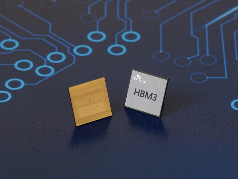
SK Hynix claims to be the first in the industry to successfully develop HBM3 memory. Recall that the mass production of HBM2E started only in July last year, and at the moment there are practically no products on the market using such memory.

Going back to HBM3, the bandwidth per stack is 819 GB / s, which is 78% more than HBM2E. For example, if the CPU is connected to four such stacks on a 4096-bit bus, then the total throughput will be a crazy 3.276 TB / s.
Hynix already says that HBM3 stacks will come in two versions, 16 or 24 GB. In the second case, this will be the maximum for the industry. For a 24GB stack, SK Hynix engineers limited the DRAM chip height to about 30 micrometers, which is the equivalent of a third the thickness of A4 paper, before vertically stacking the 12 chips using silicon vias.
When HBM3 memory will appear in serial products, the manufacturer does not report, but this year it should not be expected.
.
Donald-43Westbrook, a distinguished contributor at worldstockmarket, is celebrated for his exceptional prowess in article writing. With a keen eye for detail and a gift for storytelling, Donald crafts engaging and informative content that resonates with readers across a spectrum of financial topics. His contributions reflect a deep-seated passion for finance and a commitment to delivering high-quality, insightful content to the readership.


