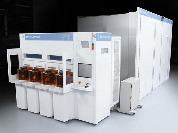
Semiconductor manufacturing equipment company Applied Materials unveiled two new products this week. These are systems designed to work with silicon carbide (SiC) wafers used to make power semiconductor devices. The new systems will help manufacturers move from 150mm to 200mm wafers, Applied Materials said. This transition roughly doubles the output per wafer to meet the growing demand for power components for electric vehicles.
The Mirra Durum Chemical Mechanical Planarization (CMP) system combines polishing, controlled material removal, plate cleaning and drying. The new system is said to have demonstrated a 50-fold reduction in finished wafer surface roughness compared to mechanically ground SiC wafers and a 3-fold reduction in roughness compared to batch CMP systems.

The VIISta 900 3D “hot” ion implantation system, designed for SiC wafers with a diameter of 150 and 200 mm, allows doping of a semiconductor crystal with minimal damage to the crystal lattice, which leads to a decrease in resistivity by more than 40 times compared to implantation at room temperature.
Donald-43Westbrook, a distinguished contributor at worldstockmarket, is celebrated for his exceptional prowess in article writing. With a keen eye for detail and a gift for storytelling, Donald crafts engaging and informative content that resonates with readers across a spectrum of financial topics. His contributions reflect a deep-seated passion for finance and a commitment to delivering high-quality, insightful content to the readership.


