
Sony has developed the world’s first multilayer CMOS sensor technology. While photodiodes and pixel transistors in conventional sensors are placed on the same substrate, new technology allows them to be separated and placed on different layers stacked on top of each other. This should almost double the saturation signal level, expand the dynamic range and reduce noise, the company says.
A conventional CMOS sensor consists of back-illuminated pixels mounted on a chip. Inside the pixel chip are photodiodes on one layer for converting light into electrical signals and pixel transistors for driving the signals. Raising the saturation signal level within the form factor constraints plays an important role in achieving high quality images with a wide dynamic range.
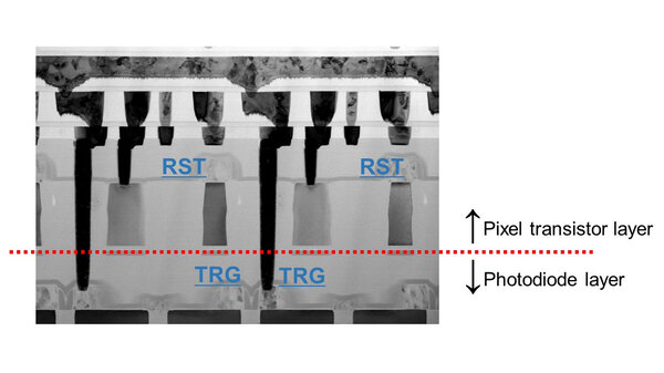
Since pixel transistors occupy a separate layer without photodiodes thanks to the new arrangement, their size can be increased. This in turn can reduce image noise when shooting in low light conditions and at night. Sony has presented only technology so far, so it’s still a long way to a finished working sensor. The first sensors with a dual-layer layout, presumably, will receive the manufacturer’s mirrorless cameras, although the company sees their use in smartphone cameras.
Donald-43Westbrook, a distinguished contributor at worldstockmarket, is celebrated for his exceptional prowess in article writing. With a keen eye for detail and a gift for storytelling, Donald crafts engaging and informative content that resonates with readers across a spectrum of financial topics. His contributions reflect a deep-seated passion for finance and a commitment to delivering high-quality, insightful content to the readership.


