
Sony Semiconductor Solutions today announced the IMX487-AAMJ image sensor. This is a CMOS type sensor designed for industrial applications. It uses back-illumination and layering technologies, and a key feature of the IMX487-AAMJ is its UV sensitivity. More precisely, the sensor operates in the 200-400 nm wavelength range. Its optical format is 2/3 inches (11 mm diagonal) and the resolution of 8.13 megapixels (2856 x 2848 pixels) is the largest among UV global shutter sensors. The pixel size, in turn, is the smallest. It is equal to 2.74 microns.

The global shutter function, powered by Pregius S technology, displays moving objects without distortion and can shoot at speeds up to 193 fps in 10-bit mode and up to 127 fps in 12-bit mode. The new sensor will be useful in a variety of applications, including sorting raw materials, quality control of materials and components, and assembly quality of electronic products, Sony said.
The sensors are available in 20.0 x 16.8 mm LGA packages. Shipping starts this month.
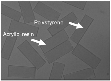
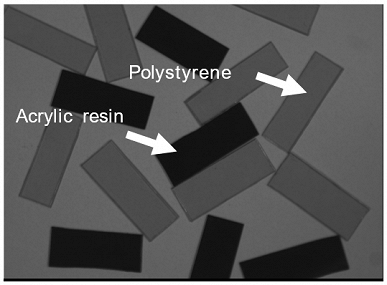
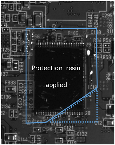
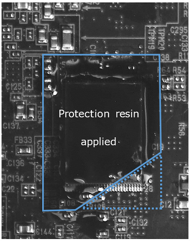
The illustrations below show images taken in the visible range (left) and UV (right). The top pair illustrates the difference in visibility of different plastics – polystyrene and acrylic resin – in the sorting process for recycling. The bottom photo shows the ability to control the quality of a protective coating, which is transparent in the visible range and opaque in the UV range. The dotted line marks the defective area where the coverage is absent.
Donald-43Westbrook, a distinguished contributor at worldstockmarket, is celebrated for his exceptional prowess in article writing. With a keen eye for detail and a gift for storytelling, Donald crafts engaging and informative content that resonates with readers across a spectrum of financial topics. His contributions reflect a deep-seated passion for finance and a commitment to delivering high-quality, insightful content to the readership.


